China’s Chipmaking Breakthrough Too Good to Be True
By Wang Jie
The Chinese internet has been abuzz recently about news of a breakthrough by Chinese scientists developing an ultra-deep ultraviolet light source for photolithography — the key process for making semiconductors. The furor was exacerbated by claims that construction of a lithography machine factory is underway in Xiongan, near Beijing.
As a science writer and academic, many people have asked me to validate this news. So let’s set the record straight: The principle of this new light source is indeed real, but it was only proposed back in 2010 — the technology is still in the proof-of-concept phase and is at least 15 to 20 years away from practical application.
Bizarrely, the source of the recent excitement was a research paper published by Tsinghua University scientists more than two years ago. Why it suddenly caught the public eye is unclear. As for the claims regarding the Xiongan factory, they are mere exaggerations.
In a nutshell: no country will be able to independently produce a lithography machine at the most advanced global standard for decades. They are the most precise and intricate apparatus that humankind has ever crafted.
And to understand the significance of these machines you needn’t look further than your everyday gadgets, from laptops and tablets to smartphones and cars — they all run on chips, which are all products of lithography.
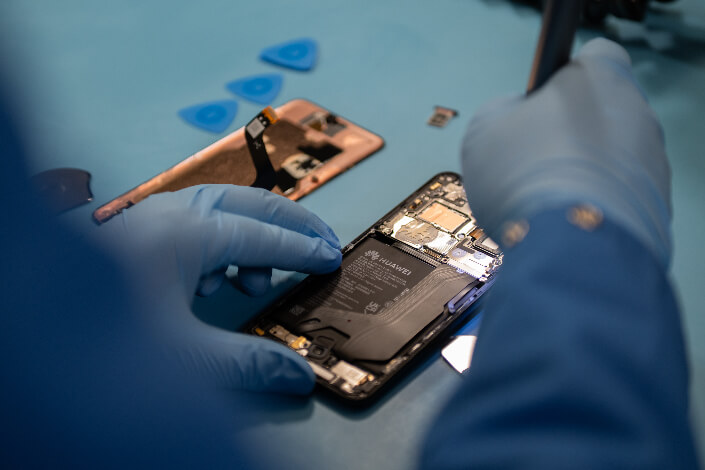
Semiconductor sophistication is measured in nanometers, indicating the size of the transistors — the smaller they are the more can fit onto a chip. For instance, the recent launch of Huawei’s new Mate 60 Pro smartphone was met with much fanfare because of speculation that it boasts a 7 nanometer (nm) chip made by China’s very own Semiconductor Manufacturing International Corp.
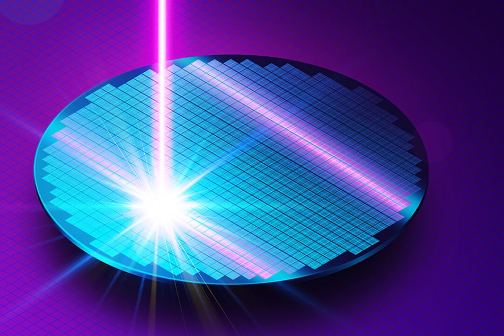
Chips are etched onto silicon wafers using lasers. The smaller you wish to etch, the shorter the wavelength of the laser needed. The world’s most advanced lithography machines utilize extreme ultraviolet (EUV) light, with a wavelength of 13.5 nm.
The Chinese scientists have supposedly created a new source for EUV light.
Originally developed by a U.S. company, which has since been acquired by Netherlands-based ASML Holding NV, EUV machines can produce 7 nm, 5 nm or even finer chips.
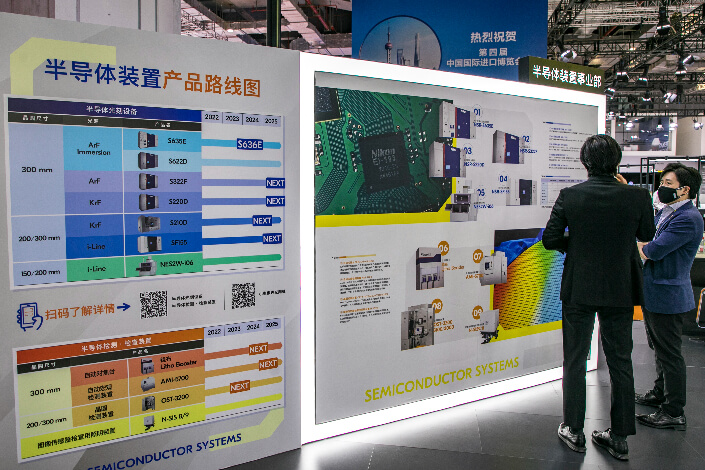
One notch below EUV is deep ultraviolet (DUV) light, which has a wavelength of 193 nm. Remarkably, the 7 nm Kirin 9000s chip in Huawei’s latest phone was produced using DUV, demonstrating the feasibility of etching 7 nm transistors with a 193 nm wavelength through a method known as multiple patterning. Currently, only a handful of global players, including ASML, Japan’s Canon Inc. and Nikon Corp., and Taiwan Semiconductor Manufacturing Co. Ltd., have mastered DUV technology.
To illustrate multiple patterning, consider a tool that can draw squares with sides of 100 mm. To draw smaller squares, you could draw a grid, shift the tool slightly, and draw again, creating overlapping lines and, therefore, smaller squares.
This method was developed for lithography and is used to produce the most advanced chips with DUV, multiple exposures are made, shifting the silicon wafer slightly between each. While this technique achieves the desired miniaturization, it’s not without challenges — the margin for error is significant.
Making a lithography machine
Just how difficult is it to manufacture a photolithography machine?
These devices consist of three primary segments: the light source, the optical system, and the etching worktable. I’d argue that creating and using each of these components is as technically challenging as landing on the moon.
Let’s start with the light source. Producing a 13.5 nm-wavelength EUV light involves firing a high-power laser at a tiny tin droplet about 30 millionths of a meter in diameter.
But such a succinct description hardly conveys the enormity of the task. Hitting the tin droplet, which is traveling at around 200 miles per hour, in order to heat it to approximately 500,000 degrees Celsius, and then hitting it again to produce the desired ultraviolet light. This sequence has to be repeated at a rate of nearly 50,000 times per second. The lasers needed for this process are so specialized that only one German company, Trumpf, has mastered its production. After a decade of research and development, they’ve produced a laser comprised of over 45,700 parts.
The optical system designed for EUV light is also monopolized by a German powerhouse: Carl Zeiss AG. While many might know Zeissfor their world-class camera lenses, their optics for EUV photolithography, in comparison, are in a league of their own, bearing a distinction akin to the difference between a propeller-driven plane and a jet fighter.
This optical system encapsulates challenges such as high-precision aspheric shaping, multi-layer reflective mirrors, top-notch smelting, ion beam polishing and ultra-precise grinding — all processes as technologically complex as their names suggest. To illustrate, the lens has to be impeccably smooth, with deviations on the atomic scale. Zeiss likens the precision to enlarging the lens to the size of Germany, with elevations no greater than 0.1 mm. A single virus on this mirror would seem like a mountain. Consequently, this system must operate in a vacuum.
Last but not least, the precision instrument worktable. Carving billions of transistors onto a silicon wafer the size of a fingernail requires an extraordinarily precise control table, constructed of over 55,000 high-precision components. These components draw on patented technologies from countries and regions including Japan, South Korea, Taiwan, the U.S., Germany, and the Netherlands. The exclusion of any one of these contributors would make the endeavor impossible.
The journey to creating the world’s most advanced photolithography machine has been arduous. After a 22-year odyssey of testing, optimization and upgrades, the first commercially viable EUV photolithography machine was finally launched in 2019.
Currently, ASML is the only company that makes the machine. The Dutch firm operates somewhat like an assembly plant at the center of an international supply chain web. Only 15% of the machine’s components are manufactured in-house, with the remaining 85% being imported.
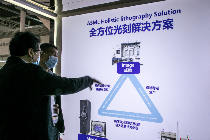
Moreover, the U.S. Department of Energy holds nearly all the core patents for the lithography machine, ASML essentially requires the Washington’s authorization to produce it. So, when the U.S. government decided to prohibit the sale of these lithography machines to China, ASML had little means to resist.
The creation of a single EUV lithography machine involves around seven or eight countries.
For China to produce lithography machines independently, it would need to achieve self-reliance and innovation across all three critical components. As of now, the only glimmer of hope is visible in creating the light source.
The research paper
In 2010, Zhao Wu, a professor at Stanford University and visiting professor at Tsinghua University, along with his doctoral students, proposed a new principle for generating an extreme ultraviolet light source.
This principle, known as “Steady-State Micro-Bunching,” or SSMB, uses a massive particle accelerator to generate the UV light. In 2017, Professor Tang Chuanxiang’s team at Tsinghua University, in collaboration with German counterparts, completed the theoretical analysis and physical design of the experiment, developed and tested the laser system, and validated some of the principle’s aspects.
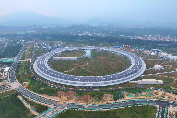
In February 2021, the team published a paper in the journal Nature. Tang’s doctoral student Deng Xiu Jie was the lead author, while Tang and a professor from the Helmholtz Berlin Center for Materials and Energy were the corresponding authors.
By March 2022, Tang and Deng had published another paper with the same title in China’s Physical Journal. I doubt they expected that about a year and half later, around Sept. 13, a Chinese self-media outlet would release a video with a rather sensational title: “Against the Heavens! Tsinghua University’s SSMB-EUV Light Source Emerges, Powering Up to 40 Times the EUV Lithography Machine.”
Following this, fueling the furor, various online platforms began to sensationalize the SSMB scheme from Tsinghua University with various headlines beginning with “Against the Heavens.” It was bewildering to witness.
But China is still a long way from producing EUV lithography machines, so let’s try and remain calm.
Firstly, as stated on Tsinghua’s website in 2021, Tang had already submitted a proposal to China’s National Development and Reform Commission to list the SSMB experimental device as a key national scientific infrastructure project during the 14th Five-Year Plan for 2021-2025.
However, I have yet to find any news about the project’s approval. Given that this is a civil research project, not a military one, such approvals usually need to be made public. Thus, as of now, it seems the project hasn’t got the green light.
If we are optimistic and imagine the project gets approved next year, I believe a scientific apparatus of this magnitude would still take at least half a decade to complete. Assuming an additional three years for successful testing and another five years to develop a commercially viable light source, 13 years would have passed. Will the other two essential components of the lithography machine be ready within these 13 years? Currently, I don’t see a hint of progress on those fronts.
Furthermore, we don’t know if in 13 years, the U.S. or the Dutch might release an even more advanced next-generation lithography machine, leaving us to play catch-up once again.
With that, I’d like to express a potentially unpopular personal opinion: Within the next 20 years, no country in the world will be able to produce a lithography machine of the most advanced global standard fully and independently. Of course, this is just my perspective, and I hope I’m proven wrong.
But while we Chinese are intelligent, we are not made of unique material that will give us the jump on the rest of humankind.
I believe that for a super-precision complex machine like the lithography machine, seeking extensive international collaboration is the best approach.
Read also the original story.
caixinglobal.com is the English-language online news portal of Chinese financial and business news media group Caixin. Global Neighbours is authorized to reprint this article.
Image: Dan74 – stock.adobe.com
